Thursday, May 20, 2010

7 segment LED programming with 8086/8088

Question
Given below is a snippet of a program that will display number “3” on a 7-segment LED which is connected at output port 08h.


Program:
MOV AL , 30h
OUT 08h, AL

7-segment detail
 7-segment LED (a-f) is connected to the port pins (1-7) respectively.
 7-segment LED is lid at low state

Assume a second 7 segment LED are connected to outport port 05h. Modify the program to display number “80” (the second LED will display number “8”).

Then assume the output from the port 05h and 08h will be inserted into another microprocessor (also at port 05h and 08h respectively). Write the program needed at the second microprocessor to receive the data. The data should be saved into any other location after retrieval.


Answer
 
30h =  011 0000 <-- gfedcba
 
a = 0
b = 0
c = 0
d = 0
e = 1
f = 1
g = 0

First LED (number 8,port 08h)
to display number 8, all will be active (active at low)

a = 0
b = 0
c = 0
d = 0
e = 0
f = 0
g = 0

000 0000 = 00h

Second LED (number 0,port 05h)
to display number 0, all will be active except g (active at low)

a = 0
b = 0
c = 0
d = 0
e = 0
f = 0
g = 1

100 0000 = 60h

therefore the complete program would be

MOV AL , 00h
OUT 08h, AL //activate first LED to display 8
MOV AL , 60h
OUT 05h, AL ////activate first LED to display 0

-------------------------------------------------

the program at the second microprocessor to receive the input

IN AL,08h // retrieve the data
MOV DL,AL // store the data at another location
IN AL, 05h
MOV DH,AL

Wednesday, May 19, 2010

Shifting & Rotating

Question
Calculate the changes in AL by each of the instruction below. (AH=33h,CF=0 and each instruction is not related to each other)
i.    RCR AL,2
ii.    SHL AL, 2    
iii.    SAR AL,2    

Answer

i.    RCR AL,2
AH=01110111 CF=0
rotate with carry to the right two times
AH = 10011101 CF=1
Answer >> AH = 9D16 CF=1

ii.    SHL AL, 2    
AH=01110111 CF=0
shift to the left two times
AH = 11011100 CF=0
Answer >> AH= DC16 CF=0

iii.    SAR AL,2    
AH=01110111 CF=0
shift arithmetic to the right two times (if the sign bit is one, then number 1 will be shifted into the stream, if not zero will be inserted, in this case the sign bit is 0 so zero will be inserted)
AH= 00011101 CF=0
Answer >> AH= 1D16 CF=0

Bus access request - HOLD,HLDA in minimum mode

Question 


In minimum mode of microprocessor 8088, HOLD and HLDA pin are used to control the bus system access by both CPU and I/O devices. Draw simplified data/wave form for HOLD, HLDA and bus access pin/device.

Answer

Bus access request - RQ/GT' maximum mode

Question

Explain how external chip/IO devices request and control the system bus in maximum mode. Draw the corresponding timing diagram.

Answer

In maximum mode, the RQ'/GT' (request and grant) pin will play the important role. Whenever a device want access to the system bus, the device will lower RQ'/GT' for one cycle to request the access. After receiving the request, 8086/8088 will grant the access to system bus by also lowering the RQ'/GT' pin for one cycle.

Note that even though it is the same pin that being lowered at both occasion, the purpose is different

Request --> RQ' = 0' = 1= requesting access
Grant --> GT' = 0' = 1 = granting access

Read cycle timing diagram in minimum mode

Question

Draw a simplified timing diagram for a read cycle of the 8088 microprocessor (minimum mode). The diagram should include at least the following
i.    Address pin
ii.    Address/Data pin
iii.    WR' pin
iv.    CLK timing
v.    ALE pin
 
 Answer

READY pin function in 8284A Clock Generator chip

Question

Briefly describe the function of READY pin in 8284A clock chip in relation to synchronization with other I/O or memory.

Answer
The ready pin generates the Ready signal for the 8086/8088. Usage example can be seen in the following READ and WRITE cycle where the important process only started after READY pin is set.


8284 Clock Generator using an external source for its frequency

Question
Modify the following  8284A clock generator circuit if it will be using an external frequency from another source.


Answer

EFI - changed from earth to the OSC input from other 8284A (EFI=external frequency input)
F/C' - changed from earth to Vcc (5v) because now the chip is using F(requency) input instead of C(rystal) input
Both X1 & X2 - grounded

Illustrated here

Calculate CLK & PCK frequency of a 8284A clock generator

Question

Given in the following diagram is a simple 8284A clock generator circuit that uses a 15MHz crystal input. Calculate the corresponding CLK and PCLK frequency. 
8284A with 15Mhz crystal diagram


Answer

CLK = 33% crystal/EFI = 0.33 (15Mhz) = 5 Mhz
PCLK = 50% crystal/EFI = 0.5 (15Mhz) = 7.5Mhz

IP and FLAG register's function

Question
What are the functions of IP and FLAG register?


Answers

Flag register - Flag register function is to record few parameter or characteristic from the last aritmetic/logic instruction. Flag register include zero flag,parity flag,carry flag,auxiliary carry flag, sign flag and overflow flag

IP register - IP is Instruction Pointer. Its function is the same as PC (program counter) in other microprocessor which is to point to the next instruction to be fetched by BIU unit to be feed into EU unit.

Monday, May 17, 2010

Read/Write bus cycle difference in minimum and maximum mode

Question
Given in the diagram below is the 8088 chip and 8288 chip connection in maximum mode. Explain the read / write difference between maximum and minimum mode operation in 8088 chip.

 Diagram: Maximum mode connection

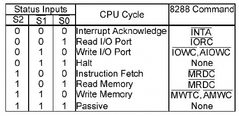
Table: 8288 Command Table
Answer
 In minimum mode, the read and write command signal are generated by 8088 using the WR' and RD' pin.

In maximum mode, the control signal to read and write are generated by external chip which is 8288. The corresponding command include MRDC' (for read) and MWTC (for write).

The following two diagram depic the difference for Read bus cycle in both minimum and maximum mode.


Difference between minimum & maximum mode from control signal perspective

Question
What is the difference between minimum and maximum mode from the control signals perspective?

Answer
In minimum mode, all control signals are self generated by 8086/8088 microprocessor such as RD' and WR'.

In maximum mode, the control signals are generated by external chip such as MRDC' (memory read) and MWTC' (memory write) by 8288 chip.

Shifting & Rotating

Question
Complete the following program so that at the end, AL will equal to FC and CF=1. Use only SHL followed by SAR AL,3 and finally RCR instruction.


MOV AL,33h // AL = 33h , initial CF=0
SHL ________
SAR AL,3 // CF-AL = 1-1111 1001
RCR ________

Answer

MOV AL,33H CF,AL : 0 0011 0011

SHL AL, 2 ; CF,AL : 0 1100 1100
SAR AL, 3 ; CF,AL : 1 1111 1001
RCR AL, 2 ; CF,AL : 0 1100 1100

Basic arithmetic assembly programming

Question

Indicate any value/data/register that has been change by every program line below

MOV BX, 0202h
MUL BL
ADD BX, ((AX))
MOV DX,ES:[0001h]
MOV [BP],CX


Answer

MOV BX, #0202h // BX = 0202h

MUL BL // AX = 0001h x 02h = 00002h

ADD BX, ((AX)) // BX = 11ABh + (0004)=11ABh + 0001h=11ACh

MOV DX,ES:[0001h] // DX =8967h

MOV [BP],CX // 50005 = 1F, 50006=CB

Arithmetic & Logic assembly programming

Question

Identify the new value of AX, BX dan CX after the program below.

MOV AX, 1234H

MOV BX, ABCDH
MOV CH, 1D
MOV CL, 255D
OR AH, 10H
AND BX , 1111000011110000b
NOT CX

Answer
 
AH  = 12h = 00010010

          10h = 00010000

AH OR AL = 00010010
--> AX = 1234h

BX = ABCD --> A0C0

CX = NOT ( 0AFF) = 1111 0101 0000 0000b = F500h

Assembly programming rules & LEA

Question

Identify the mistake in the following code, then rewrite a correct code.

LEA AX, DATA2

MOV ES:[0111h] , 1234H
ADD ES:[0111h], (AX)

Answer


The major mistake is the third line where there is an attempt to transfer data from memory location pointed by AX to another memory location in Extra Segment memory location. Memory to memory transfer is not permitted in 8086/8088 microprocessor.

An alternative code:

LEA AX, DATA2

MOV ES:[0111h] , 1234H
MOV DX,(AX)
ADD ES:[0111h],DX

Thursday, May 13, 2010

Flag Value (CF,PF,AF,ZF & CF) Tutorial

Question
State the final flag's value (CF, PF, AF, ZF & SF) for the operation given below. Explain the reason.
MOV AH, 9CH
MOV AL, 64H
ADD AH, AL

Answer
9C16 =  1001 11002
6416 =  0110 01002

AH + AL--> AH
AH = 9C16+6416 = 1 0000 00002 (number 1 is not included because the register size is only 8 bit,therefore the AH final value is 0016)

CF = 1 (got carry from D7)
PF = 1 (the number of 1 is even)
AF = 1 (got carry from D3 to D4)
ZF = 1 (because the final value is zero
SF = 0 (because the value at D15 is zero)

Stack programming tutorial

Question
Based on the following instruction, state the final value of AX,BX dan CX. Then draw the stack produce at 'PUSH CX' instruction. [Assume SS:5000h ; SP:0305h ]

 MODEL SMALL
.STACK
.STARTUP

MOV AX, 1000H
MOV BX, 2000H
MOV CX, 3000H

PUSH AX
PUSH BX
PUSH CX

POP AX
POP CX
POP BX

.EXIT
END

Answer

Final value:
AX=3000h
BX=2000h
CX=1000h

Address Data
50301    3000h
50303    2000h
50305    1000h

8284A Clock Generator Output (CLK,Ready,Reset) tutorial

Question
There are 3 output generated by 8284A clock generator that is connected into 8088 microprocessor. Explain its function.

Answer
The 8284A clock generator consist of a synchronous divide-by-three counter. It has several output including CLK,PCLK,OSC,Reset,Ready. Out of this 3 pins are connected to the 8088 microprocessor which is CLK,Reset and Ready.

CLK- This is the clock output used by the processor and other devices that directly using the processor local bus. CLK output is 33% duty cycle clock driver.
RESET- This signal is used to reset the 8086 microprocessor
READY-This signal used to indicate the readiness of the microprocessor. It will be cleared after the guaranteed hold time to the processor has been met.

Wednesday, May 12, 2010

Exchange register content using stack segment tutorial

 Question
Write a sequence of instructions to exchange two register's content using stack in assembly language?

Answer
Let say the register is AX and BX. To exchange the register's content for both by using stack it can be done by using POP and PUSH instruction. Stack behave as last in first out (LIFO).


PUSH AX // ax data will be copied into the stack, Stack pointer (SP) decreased by 2
PUSH BX // bx data will be copied into the stack 'above' ax data, Stack pointer (SP) decreased by another 2
POP AX // the data that originally came from 'bx' will be popped into AX and removed from the stack. Stack pointer added by 2
POP BX // the data that originally came from 'ax' (remember,bx data already removed from the stack) will be popped into AX and removed from the stack. Stack pointer added by 2

Extra segment's function in 8086/8088 processor tutorial

Question
What is the function of the extra segment in a 8086/8088 processor?

Answer
Extra Segment (ES) is one the the segment available in 8086/8088 microprocessor. The other segment include Data Segment (DS) , Code Segment (CS) and Stack Segment (SS).

ES is a 16-bit register containing address of 64KB segment, usually with program data. By default, the processor would use data segment from the memory whenever it is called. For example if the instruction is MOV AX, (1000h)

Address Latch Enable pin (ALE) tutorial


Question
Based on the following ALE waveform, what are the data that flow through AD0-AD7 at cycle T3 until T4.

Answer
AD-AD7 can carry both Address and Data type of data. ALE is the pin that indicate what is the type of data that currently flow through AD-AD7 pin.

ALE = 0 ( address latch disabled --> data )
ALE = 1 ( address latch enabled --> address )


At cycle T3 until T4 ALE=0 therefore the data that flowing through AD0-AD7 is Data.

Bus Interface Unit (BIU) and Execution Unit (EU) tutorial

 Question
The diagram above is the function block diagram for Intel 8088. What are the functions played by the Bus Interface Unit and Execution Unit? How both complement each other.

Answer

Both BIU and EU have their own job specification. BIU is the unit that will oversea data or operand transfer from its original source to EU. EU is the unit that handle operation execution be it arithmetic operation or logic operation.

By separating both function, both can run concurrently therefore would enable pipelining which would expediate microprocessor processing.

Tuesday, May 11, 2010

Rotating & Shifting tutorial

Question
Calculate the changes in AX and CF for each of the instruction in the program below (Assume initial CF=0)

MOV AX, F0h
SHL AH,3
SAR AH,4
RCR AH,1
OR   AH,AL

Answer

MOV AX, F0h
--> AX = 0000 0000 | 1111 0000
--> CF = 0


SHL AH,3
--> AH = 0000 0000 , shift to left 3 times will equal to 0000 0000 (no changes)
--> AX = 0000 0000 | 1111 0000
--> CF = 0


SAR AH,4
--> AH = 0000 0000 , shift arithmetic to right 3 times will make AH equal to 0000 0000 (no changes)

--> AX = 0000 0000 | 1111 0000
--> CF = 0

RCR AH,1
--> AH = 0000 0000 , shift with carry to right 1 times will make AH equal to 0000 0000 (no changes) and CF equal to zero
--> AX = 0000 0000 | 1111 0000
--> CF = 0


OR AH,AL
--> AH = 0000 0000
--> AL =  1111 0000
--> OR AH,AL --> AH = AH OR AL = 1111 0000 (F0h) --> AX = F0F0h , CF = 0


ROL AL,3
--> AL=11110000, rotate to left 3 times will make AL equal to 1000 0111 (87h)
--> AX = F087h, CF=1

Adding 64 bits of data tutorial

Question
Show how to add the following two 64 bits of data using 8088/8086 assembly programming . The final answer must be located at CX-DX combination. Then show the final value of CF,PF,ZF,SF and AF flags.

X=4322FFFFh
Y=43210001h

Answer:

     CX DX
+   AX BX
------------
     CX DX
------------

DX+BX can be done using the normal ADD DX,BX. However DX + BX might have a carry result that should be added to the following CX+AX. Therefore to ensure the carry bit (if there is a carry) is added to the following segment ADC (ADD with Carry) must be used.

So the code for this program will be

ADD DX,BX
ADC CX,AX

4322FFFF16=  0100 0011 0010 0010 1111 1111 1111 11112
4321000116 =  0100 0011 0010 0001 0000 0000 0000 00012


  0100 0011 0010 0010 1111 1111 1111 1111

+0100 0011 0010 0001 0000 0000 0000 0001
-------------------------------------------------
  1000 0110 0100 0100 0000 0000 0000 0000 = 8644000016
-------------------------------------------------

Therefore (check the second set/second command/ADC only)
SF=1 (the sign bit is number 1)
CF=0 (no carry) 
PF=0 (number of 1 is odd)
ZF=0 (result not zero)
AF = 0 (there is carry from bit 3 to bit 4)

Popular Posts

Latest Post from my Other Blog