Wednesday, May 19, 2010

IP and FLAG register's function

Question
What are the functions of IP and FLAG register?


Answers

Flag register - Flag register function is to record few parameter or characteristic from the last aritmetic/logic instruction. Flag register include zero flag,parity flag,carry flag,auxiliary carry flag, sign flag and overflow flag

IP register - IP is Instruction Pointer. Its function is the same as PC (program counter) in other microprocessor which is to point to the next instruction to be fetched by BIU unit to be feed into EU unit.

Monday, May 17, 2010

Read/Write bus cycle difference in minimum and maximum mode

Question
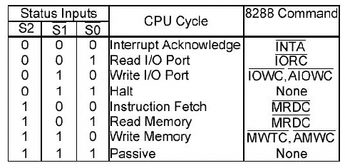
Given in the diagram below is the 8088 chip and 8288 chip connection in maximum mode. Explain the read / write difference between maximum and minimum mode operation in 8088 chip.

 Diagram: Maximum mode connection

Table: 8288 Command Table
Answer
 In minimum mode, the read and write command signal are generated by 8088 using the WR' and RD' pin.

In maximum mode, the control signal to read and write are generated by external chip which is 8288. The corresponding command include MRDC' (for read) and MWTC (for write).

The following two diagram depic the difference for Read bus cycle in both minimum and maximum mode.


Difference between minimum & maximum mode from control signal perspective

Question
What is the difference between minimum and maximum mode from the control signals perspective?

Answer
In minimum mode, all control signals are self generated by 8086/8088 microprocessor such as RD' and WR'.

In maximum mode, the control signals are generated by external chip such as MRDC' (memory read) and MWTC' (memory write) by 8288 chip.

Shifting & Rotating

Question
Complete the following program so that at the end, AL will equal to FC and CF=1. Use only SHL followed by SAR AL,3 and finally RCR instruction.


MOV AL,33h // AL = 33h , initial CF=0
SHL ________
SAR AL,3 // CF-AL = 1-1111 1001
RCR ________

Answer

MOV AL,33H CF,AL : 0 0011 0011

SHL AL, 2 ; CF,AL : 0 1100 1100
SAR AL, 3 ; CF,AL : 1 1111 1001
RCR AL, 2 ; CF,AL : 0 1100 1100

Basic arithmetic assembly programming

Question

Indicate any value/data/register that has been change by every program line below

MOV BX, 0202h
MUL BL
ADD BX, ((AX))
MOV DX,ES:[0001h]
MOV [BP],CX


Answer

MOV BX, #0202h // BX = 0202h

MUL BL // AX = 0001h x 02h = 00002h

ADD BX, ((AX)) // BX = 11ABh + (0004)=11ABh + 0001h=11ACh

MOV DX,ES:[0001h] // DX =8967h

MOV [BP],CX // 50005 = 1F, 50006=CB

Arithmetic & Logic assembly programming

Question

Identify the new value of AX, BX dan CX after the program below.

MOV AX, 1234H

MOV BX, ABCDH
MOV CH, 1D
MOV CL, 255D
OR AH, 10H
AND BX , 1111000011110000b
NOT CX

Answer
 
AH  = 12h = 00010010

          10h = 00010000

AH OR AL = 00010010
--> AX = 1234h

BX = ABCD --> A0C0

CX = NOT ( 0AFF) = 1111 0101 0000 0000b = F500h

Assembly programming rules & LEA

Question

Identify the mistake in the following code, then rewrite a correct code.

LEA AX, DATA2

MOV ES:[0111h] , 1234H
ADD ES:[0111h], (AX)

Answer


The major mistake is the third line where there is an attempt to transfer data from memory location pointed by AX to another memory location in Extra Segment memory location. Memory to memory transfer is not permitted in 8086/8088 microprocessor.

An alternative code:

LEA AX, DATA2

MOV ES:[0111h] , 1234H
MOV DX,(AX)
ADD ES:[0111h],DX

Thursday, May 13, 2010

Flag Value (CF,PF,AF,ZF & CF) Tutorial

Question
State the final flag's value (CF, PF, AF, ZF & SF) for the operation given below. Explain the reason.
MOV AH, 9CH
MOV AL, 64H
ADD AH, AL

Answer
9C16 =  1001 11002
6416 =  0110 01002

AH + AL--> AH
AH = 9C16+6416 = 1 0000 00002 (number 1 is not included because the register size is only 8 bit,therefore the AH final value is 0016)

CF = 1 (got carry from D7)
PF = 1 (the number of 1 is even)
AF = 1 (got carry from D3 to D4)
ZF = 1 (because the final value is zero
SF = 0 (because the value at D15 is zero)

Stack programming tutorial

Question
Based on the following instruction, state the final value of AX,BX dan CX. Then draw the stack produce at 'PUSH CX' instruction. [Assume SS:5000h ; SP:0305h ]

 MODEL SMALL
.STACK
.STARTUP

MOV AX, 1000H
MOV BX, 2000H
MOV CX, 3000H

PUSH AX
PUSH BX
PUSH CX

POP AX
POP CX
POP BX

.EXIT
END

Answer

Final value:
AX=3000h
BX=2000h
CX=1000h

Address Data
50301    3000h
50303    2000h
50305    1000h

8284A Clock Generator Output (CLK,Ready,Reset) tutorial

Question
There are 3 output generated by 8284A clock generator that is connected into 8088 microprocessor. Explain its function.

Answer
The 8284A clock generator consist of a synchronous divide-by-three counter. It has several output including CLK,PCLK,OSC,Reset,Ready. Out of this 3 pins are connected to the 8088 microprocessor which is CLK,Reset and Ready.

CLK- This is the clock output used by the processor and other devices that directly using the processor local bus. CLK output is 33% duty cycle clock driver.
RESET- This signal is used to reset the 8086 microprocessor
READY-This signal used to indicate the readiness of the microprocessor. It will be cleared after the guaranteed hold time to the processor has been met.

Popular Posts

Latest Post from my Other Blog